Peter Yan-Tek Hsu
MIPS Technologies, Inc.2011 N. Shoreline Blvd.
P.O. Box 7311
Mountain View, CA 94039-7311
June 2, 1994
Introduction
The R8000 project began with a vision to bring down the cost of supercomputing by an order of magnitude. In our minds supercomputers were machines that can have gigabytes of main memory and could deliver gigaflops of floating-point computation power. At the time the project was conceived in 1991, supercomputers cost millions of dollars. In other words, the going rate was several thousand dollars per megaflop. We believed that by combining mainstream microprocessor technology with supercomputer design techniques, we could create a more cost-effective supercomputer system. Our motto was "the first affordable gigaflop workstation under your desk."The magnitude of the task becomes clear when one considers that in 1991 the most advanced microprocessor achieved only tens of megaflops. We decided we could realistically get one order of magnitude performance improvement by a combination of silicon technology and processor organization, and another order of magnitude from multiprocessing. Accordingly the multiprocessor configuration was assumed from the beginning and a lot of design optimizations were made with this in mind.
Supercomputers and microprocessors evolved from a very different ancestry. Supercomputers are descendents of "general purpose data processors" with a history of numeric computing on large data sets. Microprocessors, on the other hand, descended from controllers that ran small programs in confined environments. Traditionally, microprocessors perform very well on smaller integer applications such as word processors and spreadsheets. They do not perform well when confronted with large data sets typical of the supercomputing environment.
Although supercomputers are usually characterized by their impressive floating-point compute speeds, in reality it is their memory size and bandwidth that differentiate them from other computers.To be useful, a multiply-add pair requires between one and three memory accesses to go with it. A several hundred megaflop microprocessor therefore will need a memory hierarchy that can deliver gigabytes per second of bandwidth. This kind of bandwidth is very easily provided from a little on-chip cache of, say, 16-Kbyte. However, one cannot compute for very long in a 16-Kbyte cache before exhausting all the data in it, at which time the processor must wait while the cache is refilled.
The obvious solution to attaining high bandwidth is to send loads and stores through a pipelined memory system. Unfortunately this is not desirable because accessing main memory takes a long time causing loads to have a very high latency, and such high-bandwidth memory systems are very expensive. It is well known that increasing load latencies directly impacts the execution speed of integer programs such as operating systems and compilers as well as the scalar portion of floating-point programs. These programs prefer to execute from a small, fast on-chip cache which is backed up by a large second-level cache off chip.
We designed a rather unusual "split level cache" to solve these conflicting requirements. Integer and address data resides in a small, fast on-chip cache. Floating-point data bypasses the on-chip cache and resides in a very large (up to 16-Mbyte) external cache that is somewhat slower. This external cache also acts as a second-level cache for the on-chip instruction and integer/address data cache. Hardware maintains coherence between the on-chip data cache and the external cache so there are no programming difficulties.
The split level cache scheme achieves good performance and ease of use for both supercomputer applications as well as standard workstation applications. Parallel floating-point compute-intensive applications use the multi-megabyte external cache as a "local memory" to hold blocked matrices (the external cache is set associative to make this easier). The operating system and traditional integer applications use the two level cache hierarchy in the conventional way. Coherence is maintained within each processor and across multiple processors. Programmers see a simple, flat shared virtual memory. (R8000 supports 64-bit addresses and integers.)
We envisioned R8000 microprocessors in high-end workstations and compute servers operating in a networked environment with other workstations and database servers. Binary compatibility across all platforms is essential to make such an environment friendly and productive. Most applications would be administered and stored on a single node and made available through the network. It is highly desirable for the same binary to operate on all platforms.
The binary compatibility requirement was one of the driving forces that lead us to a superscalar implementation. Vector architectures are known to work well for many floating-point applications: they are relatively simple to design, and compilers have had a long history of transforming vector loops. The disadvantages of vector architectures are that they do not scale to low-cost designs (e.g. $5000 workstations) and that the vector hardware is almost useless for general purpose integer applications. Furthermore, adding vector facilities to the MIPS instruction set would have caused a very large and traumatic change that seriously jeopardizes binary compatibility across our product line. For these reasons we reject the vector architecture approach.
Superscalar techniques provide comparable performance as vector techniques by issuing and executing multiple scalar instructions in parallel each cycle. A multiple-issue superscalar implementation of the MIPS instruction set can achieve high floating-point performance while still retaining binary compatibility with existing single-issue implementations used in lower-end workstations. With the advent of submicron silicon technology and very large dies, we felt that the logic complexity inherent in superscalar designs was a good trade-off to gain binary compatibility.
We chose to issue and complete instructions in-order in the integer pipeline because we believed that the design verification effort to validate an out-of-order pipeline would take longer and require more people than the design effort itself, a luxury we did not have. The floating-point pipeline is decoupled from the integer pipeline and supports out-of-order execution of floating-point instructions with respect to integer instructions, but the floating-point instructions themselves are issued in-order with respect to each other. Exceptions detected in the integer pipeline, such as illegal opcodes and invalid memory addresses, are precisely trapped. Exceptions detected in the floating-point pipeline, such as divide-by-zero, are normally trapped imprecisely, but for compatibility the processor supports a Precise Exception mode at degraded performance.
The initial product frequency of the R8000 chipset is 75MHz. At this frequency R8000 can issue four instructions per cycle to achieve 300 mips. Two of the four instructions per cycle can be double-precision fused multiply-add operations for a total of 300 mflops. R8000 supports two double-precision loads or stores per cycle for a cache throughput of 1.2 gigabytes per second.
This paper presents the R8000 microprocessor organization. We have attempted to highlight the more interesting features and discuss the thinking behind these design decisions. The paper begins with an overview of the processor chip set and pipeline structure. Then we discuss one of the more difficult problems in superscalar design: how to predict branches and dispatch instructions quickly enough to keep the execution units busy. After that we turn to the split level cache: interleaving for high bandwidth, hiding the latency of off-chip accesses and maintaining coherence between on-chip and off-chip caches. The paper concludes with some chip facts and performance comparisons.
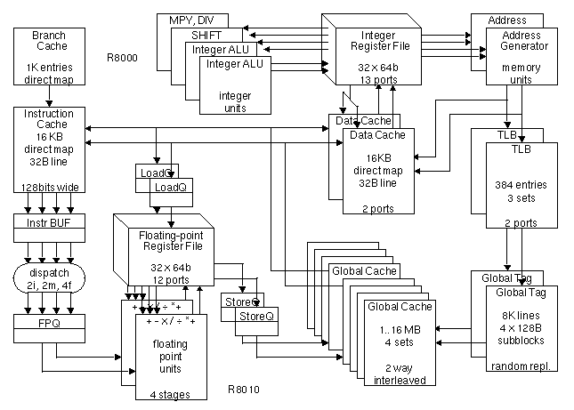
Figure 1-1: Block diagram of the R8000 microprocessor.
Processor Overview
Figure 1-1 shows a block diagram of the R8000 microprocessor. The shaded area identifies which functional units are in the integer unit (R8000) and floating-point unit (R8010) chips. Additionally, there are two tag ram chips (Global Tag) and a set of static rams making up the external cache (Global Cache).Instructions are fetched from an on-chip 16-Kbytes instruction cache (Instruction Cache). This cache is direct mapped with a line size of 32 bytes. Four instructions (128 bits) are fetched per cycle. The instruction cache is virtually indexed and virtually tagged, and is refilled from the external cache in 11 cycles. There is a branch prediction cache (Branch Cache) associated with the instruction cache. The branch cache is also direct mapped and contains 1K entries. Details of the branch cache will be discussed later.
We chose a virtually tagged instruction cache for several reasons. A physically tagged instruction cache requires that there be an associated instruction translation lookaside buffer (ITLB), which introduces a performance penalty when it misses. A virtually tagged instruction cache avoids both the logic complexity of the ITLB as well as the performance penalty of ITLB misses. Further, a virtually tagged instruction cache can improve performance by allowing the contents to not be a subset of the external second-level cache, thus avoiding displacement by data accesses that sweep the second-level cache. The complexity of physically tagged caches is usually justified on the grounds that it is easier to maintain coherence in a multiprocessing system. However, the MIPS architecture requires operating system intervention when writing into the instruction stream, so it is possible for system software to maintain coherence in instruction caches. We chose a virtually tagged instruction cache to eliminate as much complexity as possible from the instruction fetch path, which is a very critical path in the machine.
Instructions from the cache are buffered (Instr BUF) and realigned before going to the dispatch logic. Up to four instructions chosen from two integer, two memory, and four floating-point instruction types may be dispatched per cycle. Floating-point instructions are dispatched into a queue (FPQ) where they can wait for resource contention and data dependencies to clear without holding up the integer dispatching. In particular, the FPQ decouples the floating-point unit to hide the latency of the external cache. This will be discussed in more detail later.
Integer and memory instructions get their operands from a 13 port register file (Integer Register File). Integer function units consist of two integer ALUs, one shifter, and one multiply-divide unit. The ALUs and shifter operate in one cycle. The multiply-divide unit is not pipelined. The latency for 32 bit or 64 bit multiply is 4 or 6 cycles, respectively. The latency for division varies from 21 to 73 cycles depending on the number of significant digits in the result. Up to two integer operations may be initiated every cycle.
Memory instructions, which have register+offset or register+register address modes, go through the address generation units (Address Generator) and then to the translation lookaside buffer (TLB). The TLB is a three way set associative cache containing 384 entries. It is dual-ported so that two independent memory instructions can be supported per cycle. TLB misses are serviced by a software handler which uses random replacement. Integer loads and stores go to the on-chip data cache (Data Cache). It, too, is dual-ported to support two loads or one load and one store per cycle. The Data Cache is 16-Kbytes direct-mapped with a line size of 32 bytes. It is virtually addressed and physically tagged. The Data Cache is a proper subset of the external cache and hardware maintains coherence.
The Instruction Cache and Data Cache miss penalty has a very strong impact on performance, especially on integer codes which gets all of its data from the Data Cache. Both the Instruction Cache and the Data Cache refill from the external cache, which delivers 16 bytes at a time. The Data Cache refill time is 7 cycles: five to go through the external cache rams (described later) and two cycles to write the 32 byte line. The Instruction Cache refill time is longer (11 cycles) because it must be first be confirmed under branch prediction and then translated by the TLB before going to the external cache.
Floating-point loads and stores go directly off chip after translation to physical addresses and bypass the on-chip Data Cache. The external cache (Global Cache) is two-way interleaved to support two 64 bit loads or stores per cycle. It is configurable from one to 16-Mbytes in size. The external cache is four-way set associative, each cache line containing four sectors or subblocks each with its own state bits. The line size is configurable as 128, 256, or 512 bytes which corresponds to sector sizes of 32, 64, or 128 bytes, respectively. The external cache is implemented using a pair of custom tag rams (Global Tag) and from 8 to 36 commodity synchronous static rams depending on their width. The rams operate at the same frequency as the processor. Global Cache refill time depends on the system implementation.
The floating-point unit contains two execution datapaths each capable of double precision fused multiply-adds , simple multiplies, adds, divides, square-roots, and conversions. A twelve port register file (Floating-point Register File) feeds the execution datapaths, which are themselves fully bypassed. Short operations comprising compares and moves take one cycle. Medium operations comprising adds, multiples, and fused multiply-adds take four cycles and are fully pipelined. Long operations comprising divides and square-roots are not pipelined. Single and double precision divides take 14 and 20 cycles, respectively. The two datapaths are completely symmetric and indistinguishable to software--the compiler simply knows that it can schedule two floating-point operations per cycle. When one of the datapaths is busy with a non-pipelined operation, the other datapath can still execute one pipelined operation per cycle.
R8000 implements a superset of the MIPS R4000 64-bit instruction set. Future MIPS microprocessors will incorporate these instructions. There are three categories of new instructions: fused multiply-add, register+register addressing mode, and conditional moves. The fused multiply-add instructions have three input operands and performs a multiplication followed by an addition with no intermediate rounding. These instructions are available in both single and double precision. The register+register addressing mode is supported for floating-point loads and stores to enhance the performance of array accesses with arbitrary strides. A full complement of both integer and floating-point conditional moves that tests both integer and floating-point conditions were added, and the floating-point status register was extended to include a total of eight floating-point conditional code (cc) bits which can be individually set by comparison instructions. The compiler use conditional move (cmove) instructions to transform simple if-then-else constructs into straight-line code to reduce the frequency of branch misprediction. For example, the Fortran statement
if (A(i).gt.big) idx=ifload %f2=A[%r1] -- i in %r1
cmp.gt %cc1=%f2>%f1 -- big in %f1
cmove 2=%r1?%cc1 -- idx in %r2Integer Pipeline
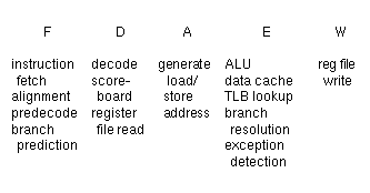
The integer pipeline is shown in Figure1-2. The Fetch stage accesses the instruction cache and the branch prediction cache (to be explained later). The Decode stage makes dispatch decisions based on register scoreboarding and resource reservations, and also reads the register file. The Address stage computes the effective addresses of loads and stores. The Execute stage evaluates the ALU operation, accesses the data cache and TLB, resolves branches and handles all exceptions. Finally, the Writeback stage updates the register file.Figure 1-2: Integer pipeline
This pipeline differs from the traditional RISC pipeline in two ways:
there are actually four pipelines--two integer ALU pipelines and two
load/store pipelines, and ALU operations occur in parallel with data cache
accesses. The traditional RISC pipeline has a load shadow; the instruction
cycle immediately after a load cannot use the result of the load. This was
found acceptable for scalar pipelines because the compiler can frequently
put some independent instruction after a load. However, the compiler would
have to find four independent instructions to cover the same shadow in
this superscalar pipeline, a rather unlikely scenario.
By delaying the ALU we remove the load shadow for load to ALU
operations but create an ALU shadow for load addresses. There is an extra
cycle of delay when an address calculated by an ALU instruction is used as
the base address by the following load or store instruction. We found this
trade-off to be advantageous because load-use dependencies occur more
frequently than compute-load/store address dependencies, particularly in
integer code with many branches which are not amenable to superscalar
speedup. In addition, the new register+register addressing mode for
floating-point loads and stores will help reduce the need for
precalculated addresses. A disadvantage of putting the ALU further down
the pipeline is that it adds an extra cycle to branch resolution. However,
many conditional branches test the result of a load, and in the
traditional RISC pipeline the extra cycle would have appeared as a load
delay slot that may not be filled. We further mitigated branch penalties
by using branch prediction to statistically hide the latency of branch
resolution.
The integer pipeline includes a number of features to enhance parallel
instruction execution. The MIPS instruction set defines all branches to
have one delay slot after it. R8000 will execute the branch and its delay
slot in parallel unless prevented by dependencies or lack of resources.
The dual-ported Data Cache includes a bypass circuit so that the common
case of a store followed by a possibly dependent load instruction can be
executed in parallel. Hardware detects the matching addresses and enables
the bypass at the byte level. Making the bypass handle all combinations of
partial word stores and loads adds some logic to the datapaths but
significantly simplifies the control logic--a good trade-off in this case.
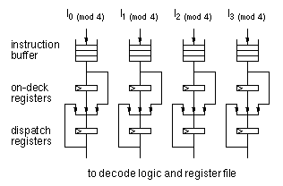
Conceptually what we need for alignment-free dispatching is a queue
that can enqueue four aligned instructions and supports dequeueing 0, 1,
2, 3 or 4 instructions per cycle. Such a structure can be implemented in a
straightforward manner as an 8-ported RAM but would be very expensive in
area. We designed an instruction queue that takes advantage of the fact
that the incoming instructions are naturally aligned on 128-bit boundaries
and that the outgoing instructions are always contiguous, shown in Figure
1-3. Quadword aligned instructions are fetched from the cache and come
in the top of the queue. The dispatch registers function as the
traditional "instruction register" connected to decoders and register
files. These registers can either be recirculated, filled from the on-deck
registers, or filled from the output of the instruction buffers. The
on-deck registers are essentially the last entry in the instruction
buffer. Their purpose is to provide access to the last two entries of the
buffer. The instruction buffer itself contains a bypass so that there is a
direct path from the instruction cache to the dispatch registers.
Figure
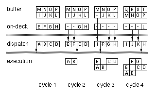
1-4 illustrates the operation of the instruction queue. Assume that
all the various registers and buffers are filled with instructions named
by letters. In cycle 1 the dispatch logic determines that out of the first
four potentially parallel instructions, only A and B can be executed
Figure 1-3: Instruction alignment and dispatch
simultaneously. (Perhaps instruction C is dependent on A, which would
also preclude D since we preserve in-order dispatching.) Signals from the
dispatch logic tells the multiplexors to move instructions E and F from
the
Figure 1-4: Example of unaligned dispatching
on-deck registers to the dispatch registers while holding instructions
C and D as shown in cycle 2. At this time the program counter points to C
as the leading instruction, and priorities are assigned starting from
there and wrapping around.
Cycle 3 illustrates how the fetch pipeline is decoupled from the
dispatch decision logic. When instructions C, D and E are replaced by G, H
and I, the on-deck registers are depleted. This event causes the buffer to
advance filling all four on-deck registers and the instruction cache to
fetch four new aligned instructions into the buffer. However, these
actions occur in the next cycle so that the critical paths involving
dispatch decisions need only manipulate the multiplexors feeding the
dispatch registers. Cycle 4 shows the simultaneous advancement of the
buffer and filling of dispatch registers to achieve continuous
alignment-free instruction dispatching.
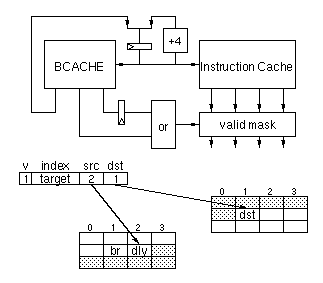
Figure 1-5: Branch prediction
instruction cache--thus eliminating almost all conflicts. Even so the
branch prediction cache takes only about half the area of the instruction
cache tags.
Figure
1-5 shows a block diagram of the instruction cache and branch
prediction cache, a sample entry from the BCACHE, and an example of
prediction. The Instruction Cache and the BCACHE are accessed in parallel
in the Fetch stage of the pipeline. The output of the BCACHE contains a
valid bit (v), the cache index of the branch target, the alignment of the
last instruction in the source basic block (src), and the alignment of the
target instruction (dst). The valid bit is set if there is a predicted
discontinuity within this quadword, and it controls the multiplexor
selecting whether the fetch program counter should be incremented by 4
instructions or loaded from the index field of the branch cache. At the
same time, the src field forms a bitmask which invalidates instructions
after the end of the basic block. The dst field is delayed one cycle and
then is used to invalidate instructions at the target quadword but before
the target instruction. Note that the delayed dst bitmask is or'ed with
the new src bitmask so that a single quadword can have both invalidations
on the left and also invalidations on the right, i.e. a very short basic
block.
One reason the branch cache takes little area is because we only store
the 10 bit cache index of the branch target as opposed to the full virtual
address of the target. We get the remaining higher-order bits of the
predicted target address from the tag of the target cache entry (recall
that the instruction cache is virtually tagged) when we fetch it in the
next cycle. This scheme implicitly assumes that all predicted branch
targets hit in the cache. While this is frequently true it does increase
the instruction cache miss penalty because miss detection cannot be
confirmed until the Execute cycle when all predictions have been resolved.
We did not explore the possibility of speculatively servicing an
instruction cache miss even before it has been confirmed because doing so
consumes valuable external cache bandwidth which we wanted to reserve for
floating-point loads and stores.
The association of a single prediction for a quadword of instructions
introduces the possibility of cache thrashing if there is more than one
branch within the quadword. (The MIPS architecture defines all branches to
include a delay slot which cannot be filled by another branch instruction.
Therefore there can be at most two branches in a quadword of
instructions.) We did not believe this was a big problem because (i)
non-taken branches do not require a prediction, and (ii) compilers can be
taught to avoid creating tiny basic blocks by using conditional move
instructions to make the small amount of code unconditionally executable.
All branches are resolved in the Execute stage of the pipeline. Because
the delay slot of branches may execute in the same cycle as the branch
instruction or be delayed by some arbitrary amount due to dependencies, we
actually associate the resolution of a branch with the delay slot of that
branch reaching the Execute stage. At that time we check the program
counter of the previous stage of the pipeline to determine whether the
branch was correctly predicted (either taken or fall through). A mismatch
between the correct program counter following the delay instruction and
the program counter in the Address Generate stage of the pipeline
indicates there has been a misprediction. Three penalty cycles are needed
to repair a branch misprediction: the pipeline is flushed, the branch
cache is updated, and fetching begins at the corrected program counter.
Our branch prediction scheme works uniformly for both the taken and
fall-through cases, and in fact also works for jump register type
instructions. Therefore we predict all types of branches and jumps
including subroutine calls and returns with the same hardware. We
originally chose this approach because it greatly simplified the pipeline
control hardware, perhaps at the expense of some performance loss.
Supprisingly we found this simple policy very effective for the emerging
object-oriented programming paradigm using dynamic shared objects where it
is common to call many small procedures indirectly via pointers. This
programming style results in many jump register type instructions whose
targets are actually invariant and thus are good candidates for branch
prediction.
A key decision was what type of RAM to use. Very roughly, there is an
order of magnitude difference in cost per bit between DRAMs and commodity
SRAMs, and between commodity SRAMs and custom SRAMs embedded in logic
chips. For example, in 1993 $250 buys 4-Mbytes of DRAM, 1-Mbytes of
commodity SRAM, or a single custom chip containing 64 to 128-Kbytes of
embedded SRAM. There are many advantages in using custom cache SRAMs:
associativity with little speed penalty, streaming buffers that support
restarting the CPU immediately after the critical word has arrived without
waiting for the rest of the cache line, high-bandwidth writeback buffer
that can evict an entire cache line from the RAM in a single cycle. The
single disadvantage of custom cache SRAMs is cost--we estimated the
external cache could only be 256 to 512-Kbytes if we used custom SRAMs.
In the end we chose to build a large external cache based on commodity
SRAMs. The deciding factor was multiprocessor cost performance. In a
uniprocessor, the higher miss rate of a smaller cache can be largely
compensated by tightly coupling the memory system and exploiting
burst-mode transfers from the DRAMs. In a multiprocessor, especially a
bus-based multiprocessor, the majority of the delay to memory is consumed
by bus arbitration and other overhead. The actual data transfer time is
only a fraction of the total delay. Therefore streaming buffers and other
overlapping techniques are much less effective in multiprocessors than in
uniprocessors. A large, multi-megabyte cache is highly desirable in a
bus-based multiprocessor because the miss rate is quite low for general
applications, typically less than 1%, and also because well-tuned code
(e.g. dividing matrices into blocks, each block being local to a single
processor) can use the large cache as a local memory to minimize
inter-processor communication. Compared to kilobyte-range caches, having
multi-megabyte caches in a multiprocessor puts much less loading on the
shared memory bus and allows more processors to be used effectively in a
single system. This improves both the total performance as well as the
cost effectiveness of the multiprocessor system by sharing main memory and
the I/O subsystem across more processors.
Having decided on commodity SRAMs, we were faced with the problem of
how to get enough bandwidth. We knew we wanted no less than a
gigabyte/second of cache bandwidth. Using 12-15ns standard asynchronous
SRAMs and taking into account address buffering and data skew, we could
cycle the SRAMs in 20-25ns and thus would need four 64-bit wide banks of
SRAMs to achieve this bandwidth. We rejected this solution as being too
expensive and mechanically too unwieldy. Instead we decided to gamble on
the Synchronous Static RAMs (SSRAM), which were in the process of becoming
standardized in 1990-91. These RAMs integrate input and output registers
onto the chip, thus pipelining the RAM access into three cycles: address
setup, RAM access, and data output. This level of pipelining was
sufficient to enable a large bank of SSRAMs to cycle at 10-12ns. Compared
to conventional asynchronous static RAMs, SSRAMs can deliver roughly twice
the bandwidth using the same basic silicon technology and I/O signals. We
expected the cost premium of SSRAMs to be perhaps 20% higher than standard
asynchronous SRAMs once they are produced in some quantity.
Using SSRAMs, we could deliver 1.2 gigabyte/second of bandwidth with
just two 64-bit wide banks of cache. The entire cache including parity
bits can be constructed with 16 or 36 RAM chips using by-9 or by-4 chips,
respectively, in a very reasonable area.
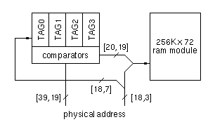
Figure 1-6: Set associative tag ram
Another key question was associativity. Our previous experiences with
multiprocessors indicated that associativity was highly desirable for
second-level caches connected to shared memory busses. Very large direct
mapped caches have the bad property that the same program may behave very
differently when re-compiled (or even reallocated in physical memory)
because minor changes in the positions of loops and subroutines can cause
huge variations in the conflict miss rate. In bus-based multiprocessors
this effect is exaggerated because the additional bus traffic slows down
other processors.
The usual way to support associativity is to read multiple banks in
parallel and then select data from the bank that hits. We rejected this
approach since it required doubling or quadrupling the bandwidth from the
cache chips. Another approach is to look up the sets serially, but we did
not use this because we wanted to access the cache every cycle. Instead we
chose to design a custom 4-way set associative tag ram as shown in Figure
1-6. The low-order bits of the physical address is used to index into
both the tag ram and the data ram. The hit information is encoded into two
bits and form the most-significant part of the address sent to the data
SSRAM.This approach gives us associativity without increasing the number
of SSRAMs. The downside is the additional latency of sequentially looking
up the tag ram in series with accessing the data rams and, of course, the
cost of the tag rams. We believed this was a good trade-off since the
external cache is used for less latency-sensitive data. The tag rams are
moderately dense custom static RAM chips: approximately 256-Kbit to
support a 4-Mbytes cache, 1-Mbit to support a 16-Mbytes cache.
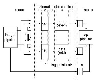
Figure
1-7 shows the external cache pipeline. Since there are two bands,
addresses are sorted into odd and even doublewords within the R8000. There
are five stages in the external cache pipeline. Addresses are sent from
the R8000 to the tag ram in the first stage. The tags are looked up and
hit/miss information is encoded in the second stage. The third stage is
used for chip crossing from the tag ram to the data rams. The SSRAM is
accessed internally within the chip in the forth stage. Finally data is
sent back to the R8000 and R8010 in the fifth stage. We allocated a full
cycle to chip crossing because TTL drivers with significant loading at 75
MHz require almost an entire cycle, and also because we wanted the
chip-set to scale well to higher frequencies.
Figure 1-7: External cache pipeline
The compiler can mitigate bank conflicts by careful code generation.
For example, it knows that references to A[i] and A[i+1] will be to
different banks of the cache. The problem arises when a subroutine with a
loop references two different arrays A[] and B[] that are formal
parameters. Because the compiler does not know what the base addresses of
the arrays are, it cannot tell if references A[i] and B[i] will go to the
same bank.
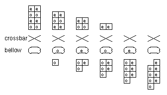
We designed hardware to help out the compiler by adding a one-deep
queue called the "address bellow." Referring to Figure
1-7, the logic immediately following the integer pipeline consists of
a crossbar for sorting even and odd references, and a register which forms
the address bellow. Figure
1-8 illustrates the operation of the address bellow. Imagine a
sequence of pairs of both even references and both odd references as
shown. Without the address bellow the interleaved cache would only be able
to process one half of a pair of references per cycle--the pipeline would
be stalled every other cycle and so the machine would run at 50%
efficiency. The purpose of the address bellow is to slightly reorder the
reference pattern so as to improve the chances of even and odd references
lining up in time. For example, the second even reference is enqueued in
the address bellow and paired with the first odd reference from the next
cycle, and so forth. We provided the address bellow to solve the local
misalignment problem; the compiler is responsible for solving the global
even/odd address mix problem. This has turned out to be a happy compromise
between silicon area (and complexity) versus software complexity.
Figure 1-8: Effect of address bellow
We chose to hide the external cache latency by decoupling the R8010
from the R8000 pipeline. Referring to Figure
1-7 , floating-point instructions are dispatched into a queue before
going to the R8010. If a floating point load instruction is immediately
followed by a compute instruction that uses the result of the load, the
queue allows both instructions to be dispatched together as if the load
had no latency at all. The integer pipeline is immediately free to
continue on to other instructions. The load instruction proceeds down the
external cache pipeline and deposits the load data in the load data queue
after five cycles. In the mean time the compute instruction waits in the
floating-point instruction queue until the load data is available.
By decoupling floating-point operations we achieve out of order
execution of floating-point instructions with respect to integer
instructions, thereby hiding the latency of the external cache. This
limited form of out-of-order execution is an example of the 80/20 rule: we
got most of the benefit of out-of-order execution while incurring only
small amounts of extra complexity. In particular, by issuing instructions
using first-in-first-out queues instead of a more general priority queue,
we avoided a lot of verification efforts because the order of
floating-point instruction execution is easily predictable. This is
important because time needed for design verification quickly becomes a
bottleneck in complex processors.
A consequence of decoupling the floating-point unit from the integer
pipeline is that floating point exceptions become imprecise with respect
to integer instructions. We briefly considered various schemes to achieve
precise exceptions but quickly decided that they were too complicated to
meet our development schedule. R8000 reports floating-point exceptions as
an asynchronous interrupt some time after the event has occurred.
Floating-point interrupts can be confined to arbitrary small regions of
the program by periodically reading the floating-point status register,
which has the side effect of flushing out all pending floating-point
interrupts. For backward compatibility we provide a Precise Exception mode
which stalls the integer pipeline whenever a floating-point instruction is
being executed, thus making all the floating-point exceptions precise.
One simplifying factor is that the external cache has very high write
bandwidth, two 64-bit doublewords per cycle, for floating-point stores. We
take advantage of this by making the on-chip integer data cache
write-through. Complexity is minimized because there is no need for a
write buffer between the on-chip cache and the external cache: the
external cache can absorb write-through at full bandwidth. Making the
on-chip cache write-through greatly simplifies multiprocessing support
because we can invalidate lines from the on-chip cache at any time without
worrying about write backs. However we did have to limit the on-chip cache
to one store per cycle because there were not enough pins on the R8000 to
write through more than one doubleword per cycle. Write-through traffic
from the on-chip cache also blocks floating-point loads and stores, but we
felt this performance penalty was acceptable because integer stores tend
not to occur in highly-optimized loops that demand maximum floating-point
load/store bandwidth.
The external cache uses a write-back policy to conserve bandwidth on
multiprocessor busses. This means that the cache tags must be interrogated
before stores are allowed to complete. This is implemented by two sets of
address and data queues, one address and data pair for each bank of the
cache. Stores are deferred in these queues while the cache tags are looked
up and are released only if they hit in the cache.
One of the unique problems introduced by a split level cache is the
coherence of integer and floating-point data. The problem is that while
integer loads and stores access both the on-chip and external caches,
floating-point loads and stores only access the external cache. For
example, if a particular memory location is first written using an integer
store, then rewritten using a floating-point store, a subsequent integer
load would get stale data (from the integer store) unless something
special was done.
The obvious solution is to invalidate the enclosing cache line from the
on-chip cache whenever a floating-point store occurs. This preserves
correctness but can lead to very poor performance. Consider the following
example of C code:
We solved this problem by attaching a valid bit to each 32-bit word
within all on-chip cache lines. Integer stores of size 32 or 64 bits will
set the corresponding valid bits, while floating-point stores will clear
them. Integer stores smaller than 32 bits (e.g. bytes) require that the
corresponding valid bit be on, otherwise it triggers a miss. Filling a
line sets all the valid bits. Having finer granularity valid bits allow
the above mentioned example cache line to both reside on chip and not
contain floating-point data. This solution solves both the performance
problem of mixed integer/float structures as well as the correctness
problem of unions containing both integer and floating-point fields.
Hsu holds a BS degree in computer science from the University of
Minnesota and MS and PhD degrees from the Univeristy of Illinois at
Urbana. He is a member of IEEE.
Alignment-Free Instruction Dispatching
One of
the early goals of the project was to design the superscalar instruction
dispatching logic such that it was as insensitive to instruction alignment
as possible. Several of us have experienced either hand coding or
designing compiler code generators for other processors where superscalar
dispatching was possible only if the instructions were aligned on
doublewords or quadwords. These experiences taught us that while alignment
restrictions were tolerable for innermost loops and other finely tuned
code fragments, such restrictions made it very inefficient to issue, in
parallel, ordinary scalar code because so much instruction padding with
nops was required that it caused excessive instruction cache misses and
other second-order effects.
Predicting Branches
The instruction cache must
fetch four instructions every cycle to maintain a dispatch rate of four
instructions per cycle. To sustain this rate in the face of branches we
must predict discontinuity in the instruction stream. We evaluated several
well-known branch prediction algorithms for layout size, speed and
prediction accuracy. We found that the biggest factor affecting area was
the infrastructure required to support a custom block: power ring and
power straps to the ring, and global routing between the branch prediction
cache and its control logic. Speed was a problem with tag comparisons for
those schemes that are associative. Accordingly we chose a simple
direct-mapped, one-bit prediction scheme which can be implemented entirely
with a single-ported RAM. This approach is advantageous in that there is
almost no speed impact and the layout can share infrastructure with the
single-ported instruction cache and tag RAMs. To make up for the low
prediction accuracy of a one-bit scheme we made the branch prediction
cache very large--one entry per four instructions in the
External Cache Organization
Thus far we have
concentrated on the integer part of the machine. Now we turn to the
floating-point part of the machine. Central to floating-point performance
is load/store bandwidth and cache size. R8000 supports an external cache
configurable from one to 16 MBytes. This cache directly feeds the R8010
and serves as the "local memory" in a multiprocessor system. A great deal
of the micro-architecture was developed to optimize the cost and bandwidth
of this external cache.
Resolving Conflicts in Interleaved
Cache
Interleaving the external cache doubles the available
bandwidth from the cache. However, it also introduces the potential for
two simultaneous references both wanting to use the same bank of the
cache. This is called "bank conflict" in traditional interleaved memory
terminology.
Decoupling the Floating Point Unit
The
five-stage external cache pipeline presents a problem for floating point
codes: a straightforward implementation would have floating-point loads
casting a shadow at least five cycles or 20 instructions long. Very
aggressive code scheduling by a compiler can perhaps cover this shadow in
loops, but scalar performance would suffer. Furthermore, code scheduled
for such long load delays would run less efficiently on existing MIPS
microprocessors such as the R4400 because the many instructions in load
delay slots cannot be run in parallel as on R8000. One of the main markets
of R8000 is as a compute server in a network environment. Interoperability
with workstations is very important: both instruction set compatibility as
well as "performance compatibility" is required. We felt we would
seriously degrade the appeal of R8000 if taking a workstation code and
recompiling it for R8000 causes that R8000 optimized code to run
significantly slower on the workstation.
Coherence in Split Level Cache
One of the most
difficult aspects in designing processors is handling stores. The split
level cache is particularly complex because coherence must be maintained
between the on-chip cache and the external cache. Furthermore, R8000
supports multiprocessing and so must implement snoop operations.
Here we have a structure containing both integer and
floating-point data lying within the same cache line. The program first
accesses some integer character data which causes the cache line to be
brought on chip. Then there is a floating-point store which knocks the
line out. The reference to some other integer data causes another cache
miss to bring the line back on chip. Mixed integer and floating-point
structures are common, particularly in graphics application, and so this
kind of thrashing cannot be tolerated.
struct { if (s.Ch[2]==...){
char Ch[4]; s.Flt =...
float Flt;
int Ival; ...= s.Ival;
} s;Conclusions
This paper described the design of
the R8000 microprocessor and highlighted some of the more innovative
features. The integer pipeline without load delay slot eliminates load-use
interlocks. The store-load bypass in the data cache allows potentially
dependent memory operations to issue in parallel. Code density is
preserved by the alignment-free instruction dispatching mechanism that
does not require nop instruction padding to achieve high issue rate. The
split level cache structure fetches large floating-point array reference
streams from the external cache into the processor without thrashing the
on-chip cache. Interleaved cache bandwidth is enhanced by the address
bellow mechanism that reorders conflicting accesses. A limited form of
out-of-order execution with register renaming is supported by decoupling
the floating-point unit from the integer pipeline. These features are
brought together to form a powerful superscalar processor.
Acknowledgment
R8000 is a collaborative
development of Toshiba Corporation, Weitek Corporation, and MIPS
Technologies Inc., a subsidiary of SGI. The author acknowledge the
contributions of the engineers and support staff from all three companies
who worked very hard to make this project successful. The result is a
credit to their skill and dedication.
Related Literature
Peter Y.-T. Hsu is an engineering director at SGI.
He helped to define the R8000 microarchitecture and managed the
development of the processor. His interests are in computer architecture,
compiler design, and VLSI design tools.